|
2.

|
Electricity/physics example
|
|
Art. 78, 83; R. 27
Description of invention
|
| [MOSFET switch for an inductive load] | |
Title of invention (designation in Request for Grant suffices)
|
|
The present invention relates to a circuit arrangement having a power MOSFET and an inductive load that is connected, first, to the source terminal of the MOSFET and, second, to a terminal having a fixed potential, and a series circuit composed of a Zener diode and of a controllable switch connected between the gate terminal of the MOSFET and the terminal.
|
R. 27(1)(a)
Technical field to which invention relates
|
|
Such a circuit arrangement has, for example, been disclosed by European Patent No. x xxx xxx. For an activated inductive load, deactivation of the inductive load is initiated by turning on the controllable switch. The latter discharges the gate-source capacitance of the power MOSFET that thus begins to turn off. The current through the inductive load initially continues to flow and builds up a voltage in a non-conducting direction at the Zener diode that can reach the Zener voltage. The driving voltage at the inductive load is therefore the Zener voltage plus the voltage drop across the controllable switch plus the gate-source voltage at the power FET. The driving voltage at the inductive load can therefore essentially be set on the basis of the selection of the Zener voltage. The magnetic energy is then quickly reduced for a high Zener voltage.
|
R. 27(1)(b)
Relevant prior art with citations
|
When the power MOSFET is operated by an electronic switch, its gate terminal lies at zero volts in a turned-off condition. When the voltage at the inductive load is reversed, the power MOSFET can begin to switch on when its emitter potential has fallen below zero by the threshold voltage. The driving voltage at the inductive load is therefore limited to a value that corresponds to the threshold voltage of the power MOSFET. The magnetic energy in this case is therefore only slowly reduced.
|
The object of the present invention is to improve a circuit arrangement of the type set forth such that a turn-on of the power MOSFET is reliably prevented as long as the voltage across the Zener diode in a non-conducting direction lies below the Zener voltage.
|
R. 27(1)(c)
Technical problem to be solved
|
|
This object is achieved by a controllable resistor connected between the gate terminal and the source terminal, the value of resistance thereof being controlled such that it has a first, high value given a current flowing upon breakdown of the Zener diode and has a second, lower value below this current.
|
R. 27(1)(c)
Disclosure of invention
|
Further developments of the invention are the subject-matter of the dependent claims.
|
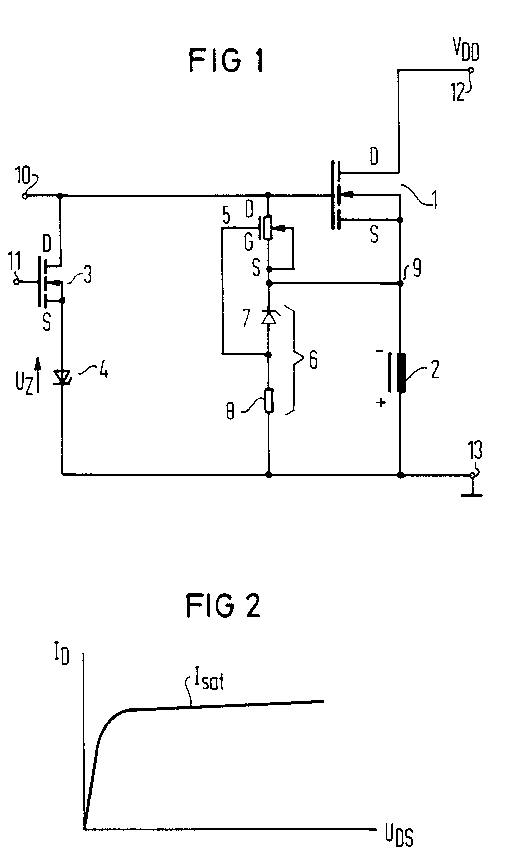
The invention is elucidated by reference to an embodiment in conjunction with FIG 1 and FIG 2. FIG 1 is a circuit diagram of the present invention; FIG 2 is a graph depicting the U/I characteristic of a controllable resistor.
|
R. 27(1)(d), (e)
Description of at least one way of carrying out invention with reference to drawings
|
The circuit arrangement of FIG 1 contains a power MOSFET 1 to which an inductive load 2 is connected in series at the source side. Via two terminals 12, 13, the series circuit is connected to an operating voltage VDD. The terminal 13 lies at a fixed potential, for example at ground. A series circuit composed of a MOSFET 3 and a Zener diode 4 is connected between the gate terminal of the power MOSFET 1 and the terminal 13. The Zener diode 4 is polarised such that it is loaded in a non-conducting direction by the driving voltage that arises from deactivation of the inductive load 2. The gate terminal of the power MOSFET is connected to a terminal 10, and the gate terminal of the MOSFET 3 is connected to a terminal 11.
An n-channel depletion MOSFET 5 is connected between the gate terminal and the source terminal of the power MOSFET 1. The source terminal of the depletion MOSFET 5 is connected to its substrate. Its gate terminal is connected to the tap of a voltage divider 6 that is connected in parallel with the inductive load 2. The voltage divider 6 is composed of a Zener diode 7 and of a resistor 8. The Zener diode 7, however, can also be replaced by a resistor.
For activating the inductive load 2, a positive voltage that is higher than the operating voltage VDD is applied to the terminal 10. It can be supplied for example by a known pump circuit.
When the inductive load is to be deactivated, the controllable switch 3 is turned on by a voltage applied to the terminal 11. The gate-source capacitance of the power MOSFET 1 is thus discharged and the power MOSFET begins to turn off. A voltage having the indicated polarity builds up at the inductive load 2. The voltage at the source terminal of the power MOSFET 1 (node 9) thus becomes negative relative to its gate voltage since its gate lies at zero volts via the terminal 10. The power MOSFET 1 could thus be switched on again.
This is prevented by the depletion MOSFET 5. This is connected as a current source; its source terminal is connected to the substrate. It is dimensioned such that its saturation current Isat (FIG 2) is higher than the reverse current that flows through the Zener diode 4 when the latter has not yet broken down. The saturation current, however, is lower than a current that would flow given breakdown of the Zener diode 4.
The voltage across the inductive load 2 after the activation of the MOSFET 3 and the turn-off of the power MOSFET 1 initially drives a current through the Zener diode 4, the MOSFET 3 and the depletion MOSFET 5 that is lower than the saturation current of the depletion MOSFET 5. Only a slight drain-source voltage drop occurs. The gate terminal and the source terminal of the power MOSFET 1 are thus situated at practically the same potential, so that it remains turned off. When the voltage at the inductive load 2 continues to rise, the Zener voltage UZ of the Zener diode 4 is reached and the Zener diode breaks down. The current driven through the Zener diode 4, the MOSFET 3 and the depletion MOSFET 5 thus increases until the saturation current of the depletion MOSFET is reached. The drain-source voltage of the depletion MOSFET thus increases and the power MOSFET 1 is activated when its cut-off voltage is reached. The current of the inductive load 2 can thus flow through the operating voltage source and the power MOSFET 1. The driving voltage is thereby defined by the voltage UZ plus the drain-source voltage of the controllable switch 3 plus the drain-source voltage of the depletion MOSFET 5. It can be set by an appropriate selection of the Zener diode 4.
In order to reliably turn off the depletion MOSFET 5 when the load 2 is activated, it must have a high resistance when a control voltage is applied at the terminal 10. This is achieved in that its gate terminal is negatively biased in comparison with its source terminal via the voltage divider 6. The depletion MOSFET 5 is thus turned off as long as the voltage at the node 9 is more positive than at the terminal 13.
The MOSFET 3 can be replaced by some other controllable switch, for example by a bipolar transistor. The depletion MOSFET 5 can also be replaced by some other controllable resistor, for example by a bipolar transistor.
|
1.
|
Circuit arrangement having a power MOSFET (1) and an inductive load (2) which is connected, on the one side, to the source connection and, on the other side, to a terminal (13) which is at a fixed potential, having a series circuit, consisting of a Zener diode (4) and a controllable switch, which is connected between the gate connection and the terminal,
|
|
R. 29(1)(a)
Prior art portion of independent claim wherever appropriate
|
|
characterised by a controllable resistor between the gate connection and the source connection, the resistance of which is controlled such that it has a first, high value when a current flows at breakdown of a Zener diode and, below this current, a second, lower value.
|
R. 29(1)(b)
Characterising portion
|
|
2.
|
Circuit arrangement according to claim 1,
|
|
R. 29(3), (4)
Dependent claim
|
characterised in that the controllable resistor is a current source, the current of which is smaller than the current flowing at Zener breakdown.
|
3.
|
Circuit arrangement according to claim 2,
|
|
characterised in that the current source is a depletion FET (5), the saturation current of which is smaller than the current flowing at Zener breakdown.
|
|
4.
|
Circuit arrangement according to claim 3,
|
|
characterised in that the gate connection of the depletion FET (5) is connected to the tap of a voltage divider (6) which is connected in parallel with the inductive load (2).
|
| MOSFET switch for an inductive load | |
R. 33(1)
Title of invention
|
|
In order to rapidly reduce the magnetic energy of an inductive load (2), the driving voltage must be high. When the load (2) is disconnected via a MOSFET (3) operating as a source follower, then a premature activation of the MOSFET (3) given reversal of the voltage at the inductive load (2) must be prevented. In a known manner, a series circuit of a Zener diode and of a controllable switch (3) is connected between the gate and the load (2). According to the present invention, a current source whose current is lower than the current that would flow upon Zener breakdown is connected between the gate and the source. The MOSFET (3) then becomes conductive upon Zener breakdown and the energy is quickly reduced by a high voltage, essentially by the Zener voltage.
|
R. 33(2), (3), (5)
Content of abstract
|
|

 ANNEX III Examples of European patent applications
 1. Chemistry example
 3. Mechanics example